News Center
[Dry goods sharing] The 10 most common problems in switching power supply debugging
2021-12-11
Transformer saturation
The current through the transformer (and switch tube) increases nonlinearly when the machine is started under high voltage or low voltage input (including light load, heavy load, capacitive load), output short circuit, dynamic load, high temperature, etc. When this phenomenon occurs, the peak value of the current cannot be predicted and controlled, which may lead to current over-stress and resulting switch tube over-voltage damage.
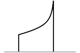
Current waveform at transformer saturation
Conditions prone to saturation:
1) Transformer inductance is too large;
2) Too few laps;
3) The saturation current point of transformer is smaller than the maximum current limiting point of IC;
4) There is no soft start.
terms of settlement:
1) Reduce the current limiting point of IC;
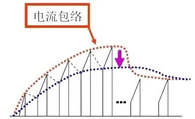
2) Strengthen the soft start to make the current envelope through the transformer rise more slowly.
2. Vds too high
Stress requirements of Vds:
Under the worst conditions (maximum input voltage, maximum load, maximum ambient temperature, power start or short circuit test), the maximum value of Vds shall not exceed 90% of the rated specification
Ways to reduce Vds:
1) Reduce the platform voltage: reduce the ratio of primary and secondary side turns of the transformer;
2) Reduce peak voltage:
A. Reduce leakage:
The main reason for the peak voltage is that the leakage inductance of transformer stores energy when the switch is turned on. Reducing the leakage inductance can reduce the peak voltage.
B. Adjust the absorption circuit:
① Use TVS pipe;
② Using a slower diode, it can absorb a certain amount of energy (spike);
③ Inserting damping resistance can make the waveform smoother and reduce EMI.
3. IC temperature too high
Causes and solutions:
1) Internal MOSFET loss is too large:
The switching loss is too large, and the parasitic capacitance of the transformer is too large, resulting in a large cross area between the opening and closing current of the MOSFET and Vds. Solution: increase the distance between transformer windings to reduce the interlayer capacitance, just as a layer of insulating tape (interlayer insulation) is added between layers when the winding is wound in multiple layers.
2) Poor heat dissipation:
A large part of IC heat is transferred to PCB and copper foil on it by pins. The area of copper foil should be increased as much as possible and more solder should be applied
3) The air temperature around IC is too high:
IC should be in a place with smooth air flow, and should be away from parts with too high temperature.
4. Unable to start with no load or light load
Phenomenon:
No load and light load can not be started, and Vcc repeatedly bounces back and forth from the starting voltage and shutdown voltage.
reason:
During no-load and light load, the induced voltage of Vcc winding is too low, and it enters into repeated restart state.
terms of settlement:
Increase the number of coils of Vcc winding, reduce the current limiting resistance of Vcc, and properly add false load. If the number of Vcc windings is increased and the current limiting resistance of Vcc is reduced, the Vcc becomes too high under heavy load, please refer to the method of stabilizing Vcc.
5. Cannot load after starting
Causes and solutions:
1) Vcc is too high under heavy load
In case of heavy load, the induced voltage of Vcc winding is high. When the Vcc is too high and reaches the OVP point of IC, the overvoltage protection of IC will be triggered, causing no output. If the voltage rises further, the IC will be damaged if it exceeds its bearing capacity.
2) Internal current limiting is triggered
A. Current limiting point is too low
Under heavy load and capacitive load, if the current limiting point is too low, the current flowing through the MOSFET will be limited and insufficient, resulting in insufficient output. The solution is to increase the resistance of the current limiting pin and increase the current limiting point.
B. The current rise slope is too large
If the rising slope is too large, the peak value of current will be larger, which is easy to trigger the internal current limiting protection. The solution is to increase the inductance without saturating the transformer.
6. High standby input power
Phenomenon:
Vcc is insufficient at no load and light load. This situation will cause the input power to be too high and the output ripple to be too large at no load and light load.
reason:
The reason why the input power is too high is that when Vcc is insufficient, the IC enters into the repeated starting state, and the high voltage is frequently required to charge the Vcc capacitor, resulting in the loss of starting circuit. If there is a resistance between the starting pin and the high voltage, the power consumption on the resistance will be large, so the power level of the starting resistance should be sufficient.
The power IC has not entered Burst Mode or has entered Burst Mode, but the Burst frequency is too high, the switching times are too many, and the switching loss is too large.
terms of settlement:
Adjust the feedback parameters to reduce the feedback speed.
7. Excessive short circuit power
Phenomenon:
In case of output short circuit, the input power is too large and Vds is too high.
reason:
When the output is short-circuited, there are many repetitive pulses, and the peak current of the switch tube is large, which causes the switch tube current with too large input power to store too much energy on the leakage inductance. When the switch tube is turned off, it causes high Vds.
There are two possible reasons for the switch tube to stop working in case of output short circuit:
1) Triggering OCP can stop the switch action immediately
A. Trigger OCP of feedback pin;
B. Switch action stops;
C. Vcc drops to IC closing voltage;
D. The Vcc rises to the IC starting voltage again and then restarts.
2) Trigger internal current limiting
When this mode occurs, limit the available duty cycle and stop the switch action depending on the Vcc falling to the lower limit of UVLO, while the Vcc falling time is longer, that is, the switch action is maintained for a longer time, and the input power will be larger.
A. Internal current limiting is triggered, and the duty cycle is limited;
B. Vcc drops to IC closing voltage;
C. Switch action stops;
D. The Vcc rises to the IC starting voltage again and then restarts.
terms of settlement:
1) Reduce the number of current pulses to trigger the OCP of the feedback pin when the output is short-circuited, which can quickly stop the switch action and reduce the number of current pulses. This means that when the short circuit occurs, the voltage of the feedback pin should rise faster. So the capacitance of the feedback pin should not be too large;
2) Reduce the peak current.
8. No load, light load output ripple is too large
Phenomenon:
Vcc is insufficient at no load or light load.
reason:
When Vcc is insufficient, the oscillating IC works intermittently between the starting voltage (such as 12V) and the turn-off voltage (such as 8V) for a long period of time, providing energy to the output for a short time, and then stopping working for a long time, which makes the energy stored by the capacitor insufficient to maintain the output stability, and the output voltage will drop.
resolvent:
Ensure that Vcc can supply stably under any load condition.
Phenomenon:
In Burst Mode, the frequency of intermittent operation is too low. This frequency is too low, and the energy of output capacitance cannot be maintained stable.
terms of settlement:
Under the condition of meeting the requirements of standby power consumption, slightly increase the frequency of intermittent operation and increase the output capacitance.
9. Heavy load and capacitive load cannot be started
Phenomenon:
Light load can be started, and heavy load can be added after starting, but it cannot be started under heavy load or large capacity load.
General design requirements:
Regardless of heavy load or capacitive load (such as 10000uF), the input voltage is the lowest or the lowest, and the output voltage must rise to a stable value within 20mS.
Causes and solutions (on the premise that Vcc is within the normal working range):
Let's take the capacitive load C=10000uF as an example for analysis,
According to the specification, there must be enough energy to make the output rise to a stable output voltage (such as 5V) within 20mS.
E=0.5*C*V^2
The larger the capacitance C, the greater the energy that needs to be transferred from input to output within 20mS.
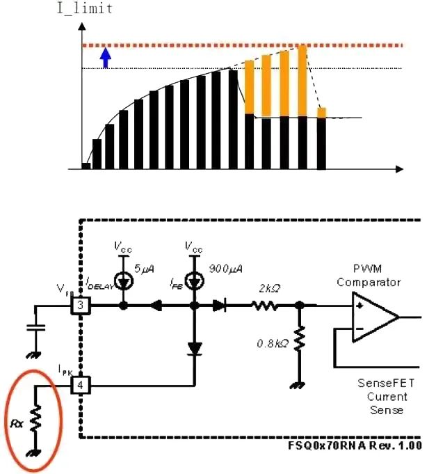
Take the chip FSQ0170RNA as an example, as shown in the figure, the total area S of the shaded part is the required energy. To increase the area S, the method is:
1) Increase peak current limiting point I_ Limit, which can allow the flow of larger inductive current Id: increase the resistance connected with Pin4, and reduce the shunt from the internal current source Ifb, so that the voltage at the positive input end of the PWM comparator as the current limit reference voltage will rise, that is, allow greater current to flow through the MOSFET/transformer, which can provide greater energy.
2) During startup, increase the time of energy transmission, that is, extend the rise time of Vfb (before reaching the OCP protection point).

For this FSQ0170RNA chip, the inductive current control takes Vfb as the reference voltage, and the waveform of Vfb voltage is proportional to the envelope of the inductive current. By controlling the rise time of Vfb, the rise time of the inductance envelope can be controlled, that is, the time of energy transfer can be increased.
The OCP function of IC is realized by detecting that Vfb reaches Vsd (such as 6V). Therefore, to reduce the slope of Vfb, the rising time of Vfb can be extended.
When the output voltage does not reach the normal value, if the feedback pin voltage Vfb has risen to the protection point, the energy transfer time is not enough. When the heavy load and capacitive load are started, the output voltage is set up slowly. When the optocoupler voltage is low, the current through the optocoupler diode is small, and the optocoupler photosensitive tube has a long time in the high resistance state (tends to turn off). The IC internal current source charges the capacitor connected to the feedback pin quickly. If Vfb rises to the protection point (such as 6V) within this time, the MOSFET will turn off. The output cannot reach the normal value, and the startup fails.
terms of settlement:
When the output voltage reaches the normal value, the feedback pin voltage Vfb is still less than the protection point. Make Vfb move away from the protection point and rise slowly, or extend the time when the feedback pin Vfb rises to the protection point, that is, reduce the rising slope of Vfb, so that the output has enough time to rise to the normal value.
A. Increasing the feedback capacitance (C9) can reduce the rising slope of Vfb, as shown in the figure, from line D to line A. However, if the feedback capacitance is too large, it will affect the normal working state, reduce the feedback speed and increase the output ripple. So the capacitance cannot change too much.
B. Due to the deficiency of method A, connect a capacitor (C7) in series with the voltage regulator (D6, 3.3V) in parallel to the feedback pin. This method will not affect the normal operation, as shown in line B, when Vfb
Notes:
1) Increasing the feedback pin capacitance (including the voltage regulator tube string capacitance) has little effect on solving the problem of super capacitive load;
2) Increase peak current limiting point I_ Limit, which also increases the OCP point under steady state. It is necessary to check whether the transformer will be saturated under capacitive load and minimum input;
3) If the current limiting point is to be maintained, R10 must be × C11 is larger, but in the case of super capacitive load (10000uF), the rise time of 5Vsb may be increased by more than 20mS. This method needs to check whether the dynamic response is too affected;
4) The bias resistance R10 of 431 is too small, and the C11 of 431 in parallel is larger;
5) To ensure the rise time, increase OCP point and R10 × The C11 method may be used at the same time.
10. No load and light load output rebound
Phenomenon:
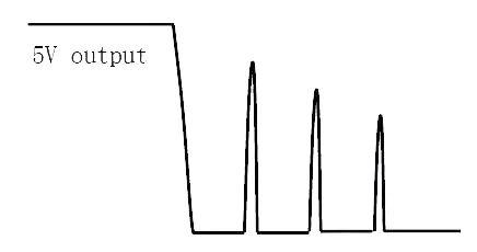
When the output is no-load or light, turn off the input voltage, and the output (such as 5V) may have a voltage rebound waveform as shown in the figure below.
reason:
When the input is turned off, the 5V output will drop, and the Vcc will also drop, and the IC will stop working. However, when the load is empty or light, the large capacitance voltage of the huge PC power supply cannot drop rapidly, and still can provide a large current to the high voltage starting pin to make the IC restart, and the 5V will output again and jump back.
resolvent:
A large current-limiting resistor is connected in series at the starting pin, which makes the large capacitor voltage drop to a relatively high level and is not enough to provide sufficient starting current to the IC.
Before connecting the start to the rectifier bridge, the start is not affected by the large capacitance voltage. When the input voltage is turned off, the starting pin voltage can drop rapidly.
Hot news

2021-12-25
Guangdong Guangxin Photoelectric Technology Co., Ltd Ending of excellent operation management projectGuangdong Guangxin Photoelectric Technology Co., Ltd In order to improve the management level of the company, better meet and serve customers, and speed up the response to customers, the company has carried out the excellent operation management project w

2021-12-15
Guangdong Guangxin Photoelectric Technology Co., Ltd Go to Jiangsu to serve customers in the East China market with LED drive power supplyGuangdong Guangxin Photoelectric Technology Co., Ltd Production and sales of LED light drive power supply (LED drive power supply), with rich product lines, mainly based in Guangdong for many years; However, there are many LED lamp manufacturers in Jiang
2021-12-11
FAQ of LED drive power supplyThe LED driver we mentioned includes digital driver and analog driver. Digital driver refers to digital circuit driver, including digital dimming control, RGB full-color change, etc. Analogue drive refers to analog circuit drive, including AC constant cur


Copyright © Guangdong Guanx Photoelectric Technology Co., Ltd All Rights Reserved 粤ICP备2021156941号-1
Website Construction:LEEKIND